Responsible
Research Area
Research Lines
Activities
The photonic devices group is active at the Dipartimento di Elettronica, Informazione e Bioingegneria of the Politecnico di Milano since 1996.
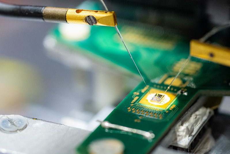
The activity is focused on photonic integrated circuits on several photonic platforms (glass, Indium Phosphide, Silicon nitride and oxynitride) in both linear and non-linear regime. The competences include electromagnetic simulations, circuit analysis, waveguides characterization and photonic devices applied to high bit rate optical communications, sensors system, and optical interconnects.
The research activities are aimed to the realization of large-scale integration photonic circuits, high performances optical waveguides by means of non-conventional optical materials, complex and reconfigurable photonic architectures using sensors and new generation optical actuators, and development of design kit for high level design of photonic integrated circuits. The group also performs research in the field of integrated optical sensors for biophotonic sensors in order to detect cancer cells, proteins and DNA.
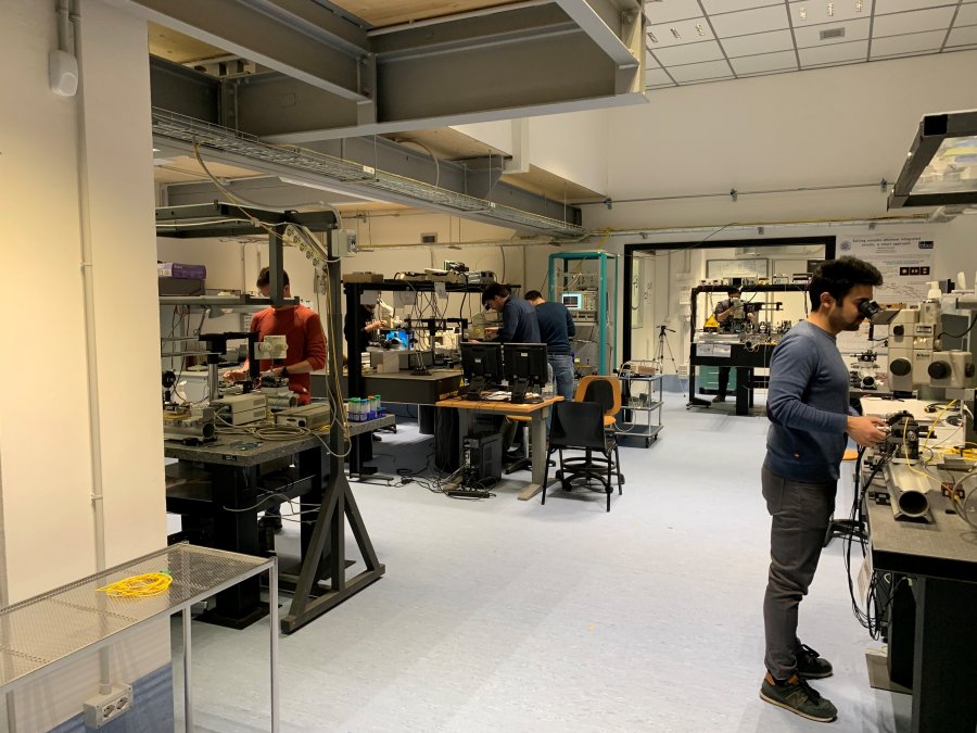
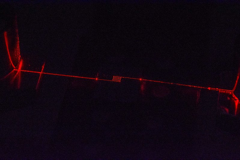
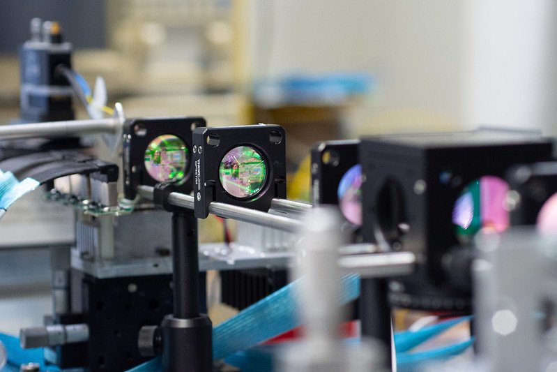
The laboratory is equipped with five optical benches, which allow performing a wide range of experimental measures on photonic waveguides and circuits, both in time and spectral domain, linear and non-linear regime.
The group has also access to the clean room of PoliFab, the new centre for micro and nano technologies of Politecnico di Milano.
Service information
The photonic devices Lab is located at the PoliFab (building 30, in Via Giuseppe Colombo 81).