Research Area:
Responsible:
Research Lines:
Project abstract
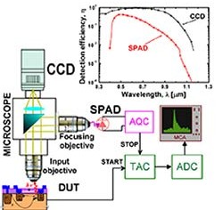
The aim of the Project is to conceive technologies and to implement methodologies for the non invasive testing of integrated ULSI (Ultra Large Scale of Integration) electronic circuits. The apparatus is based on experimental measurements of the luminescence spontaneously emitted by integrated circuits during normal operation, with time resolution of just few tens of picoseconds. Other related goals of the research are the development and validation of analytical and SPICE models for the luminescence in single MOS transistors under high electric fields, for the simulation and the experimental crosscheck of the timing behavior of both luminescence and electric signals inside the chip, by means of CAD simulations, in order to detect and identify circuital defects, failing block, or violated specifications. The research group developed and realized:
- a microscope set-up for the optical inspection of integrated circuits by means of 2-dimensional CCD (Charge-Coupled Devices) static imagers and time-resolved SPAD (Single Photon Avalanche Diode);
- some analytical models and SPICE that take into account the emitted luminescence vs. the transistor operating point and the fabrication technological parameters;
- methodologies to compare experimental measurements and CAD simulations, in order to discover and locate circuital malfunctions and failures;
- test and debug of real chips.
Currently some research collaborations are on-going with IBM, T.J. Watson Research Center, Yorktown Heights, USA, researchweb.watson.ibm.com/journal/rd/444/tsang.html Dr. Franco Stellari and STMicroelectronics – Agrate Brianza.
Project results
- “Tools for Contactless Testing and Simulation of CMOS Circuits” F. Stellari, F. Zappa and S. Cova Microelectronics Reliability, vol. 41, no. 11, 1801-1808 (Nov. 2001).
- “High-Speed CMOS Circuit Testing by 50ps Time-Resolved Luminescence Measurements” F. Stellari, F. Zappa, , S. Cova, C. Porta and J. C. Tsang IEEE Transactions on Electron Devices, vol. 48, no. 12, 2830-2835 (Dec. 2001).
- “Backside Flip-Chip testing by means of high-bandwidth luminescence detection” A. Tosi, F. Stellari, F. Zappa, and S. Cova Microelectronics Reliability, vol. 43, issue 9-11, 1169-1674, 2003.
- “CMOS Circuit Testing via Time-Resolved Luminescence Measurements and Simulations” F. Stellari, A. Tosi, F. Zappa, and S. Cova IEEE Transactions on Instrum. and Measurements, vol. 53, no. 1, 163-169, 2004.
- "Current crowding in faulty MOSFET: optical and electrical investigation" A. Tosi, F. Stellari, and F. Zappa Microelectronics Reliability, vol. 44, issue 9-11, Sep.-Nov. 2004, 1577-1581.
- "Implementation of TRE systems into Emission Microscopes" A. Tosi, M. Remmach, R. Desplats, F. Zappa, and P. Perdu Microelectronics Reliability, vol. 44, issue 9-11, Sep.-Nov. 2004, 1529-1534.
- “Innovative packaging technique for backside optical testing of wire-bonded chips” A. Tosi, F. Stellari, F. Zappa Microelectronics Reliability, Vol. 45, Issue 9-11, September - May, 2005, pp. 1493-1498.