Activities
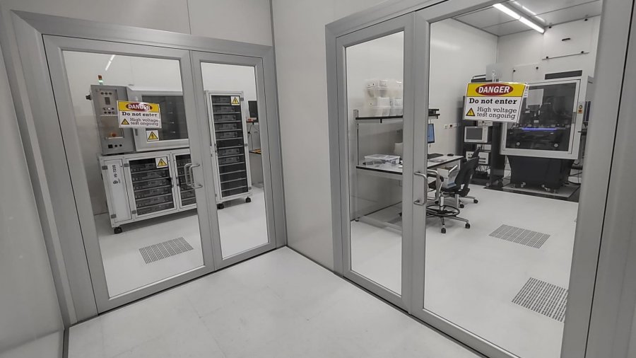
Power electronics offers today extraordinary prospects for research, industrial innovation, and social impact. The growing awareness of the importance of careful and sustainable energy management has, more than ever, expanded the market and application fields of this branch of electronics, while also stimulating its development. In this context, the Power Devices and Circuits Laboratory represents a research infrastructure active in both power devices and power circuits, with strong industrial collaborations and a mission to foster innovation across a wide range of applications. The laboratory includes an experimental area of approximately 100 sqm, certified as an ISO9 cleanroom, for electrical testing activities, and a computing room of about 50 sqm dedicated to modeling and numerical simulations.
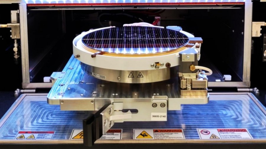
The activities of the laboratory on power devices focus on experimental and modeling studies of various types of components, with the goal of supporting the development of next-generation technologies. Special emphasis is given on devices for galvanic isolation based on polymeric materials, as well as on MOSFET, IGBT, and HEMT transistors based on Si, SiC, and GaN. Experimental analyses are carried out with advanced instrumentation that enables electrical characterizations up to 10 kV, both at the wafer level and on packaged samples. Modeling analyses are performed with a commercial semiconductor device simulator (Synopsys TCAD) or in-house software.
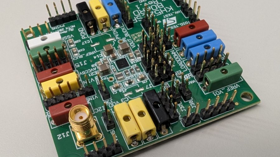
The activities on power circuits are focused on two main research areas. The first involves time-based controlled integrated DC-DC converters for both portable and industrial applications. The second focuses on resonant hybrid switched-capacitor converters. The common goal of both research areas is to increase power conversion efficiency and reduce converter costs by minimizing the area occupied on the wafer. Activities range from theoretical studies and circuit conceptualization to design and simulation, and finally to electrical testing of the developed prototypes.
Service information
The laboratory is located on the ground floor of Building 23, Via Golgi 40.