Prof. Jian Chen
Stanford University
DEIB - 21.S.4 Room (Bld. 21)
April 15th, 2024 | 11.15 am
Contact: Prof. Marco Sampietro
Research Line: Electron devices
Sommario
On
April 15th, 2024 at 11.15 am
Jian Chen, Adjunct Professor at Stanford University, will hold a seminar on "
History, Challenges and Opportunities on the Memory Lane: From 2D to 3D" in DEIB 21.S.4 Room (Building 21).
In our modern data abundant and digital world, various types of memory technologies are becoming ever more important in the memory and computing hierarchy. As an industry, we are gifted with secular and insatiable demand, demand in ever lower cost, higher density, lower power, performance, functionality, and reliability. Two types of memory dominate the landscape, NAND for low-cost storage, and DRAM for fast main computing memory.
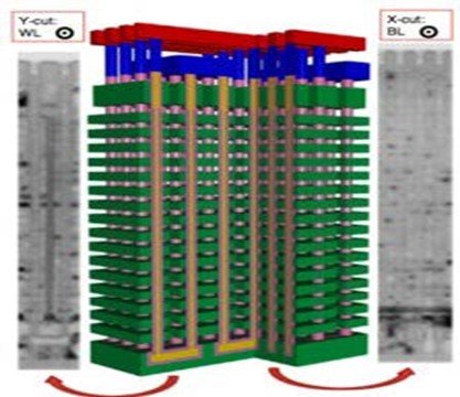
This talk will share the history and current states of the technologies, how NAND has successfully transitioned from 2D to 3D with continued scaling path, and DRAM has reached scaling bottleneck, with possible but difficult transition to 3D on the horizon.
Biografia
Currently an adjunct professor at Stanford, Jian was senior Vice President of Technology responsible for SanDisk’s 3D NAND technology development from 2013 to 2020. Prior to that, he was VP of Memory System Engineering leading exploring of emerging memory system architecture and product designs of SD/uSD, and SSD. He was the first device/process engineer to work on the SanDisk-Toshiba joint NAND venture in 1999, worked at the joint fab in Yokkaichi and built up the SanDisk organization from 2005 to 2007. With 150+ granted US patents, he invented some of the fundamental patents in NAND device/process and systems that are been used for over 10 generations of NAND products. Prior to SanDisk, he worked on 3 generations of NOR flash memory at AMD. He is co-author of a book chapter on Flash Memory Reliability and JEDEC flash memory reliability standard. He published the papers that first discovered the root cause of GIDL and coined the term GIDL. He received his MS and Ph.D. in EECS from UC Berkeley, and B.S. in Solid State Device Physics from University of Electronic Science and Technology, Chengdu, China.
Allegati

