Responsible
Research Area
Research Lines
Activities
The research laboratory is active in the field of the design of application-specific integrated circuits (ASIC) in the most modern CMOS processes at the nanoscale (today down to 28nm bulk and 22nm fully depleted SOI CMOS processes). Such technology nodes enable today digital signal processing at superior speeds, lower consumption and area occupation, but, at the same time, tend to degrade the analog block performances, such as gain, matching or noise. The full integration of high-performance electronic systems in silicon, such as those used in high-efficiency high-frequency power conversion or those used in wireless systems at radio frequency (RF) and millimeter-wave (mmW) frequencies (such as 5G wireless), and in high-spatial-resolution radar systems for autonomous vehicles, require a paradigm change in design, such that digital signal processing becomes serviceable to each analog block to improve efficiently its performances, compensating environmental variations in real time. This new approach allows to increase scalability and energy efficiency of modern CMOS integrated systems and has applications in different domains.
Scientific collaborations on those topics are already active with other universities and research centres (Intel Labs, IMEC), as well as joint-research efforts with semiconductor companies such as Infineon Technologies, STMicroelectronics.
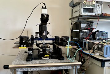
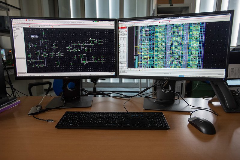
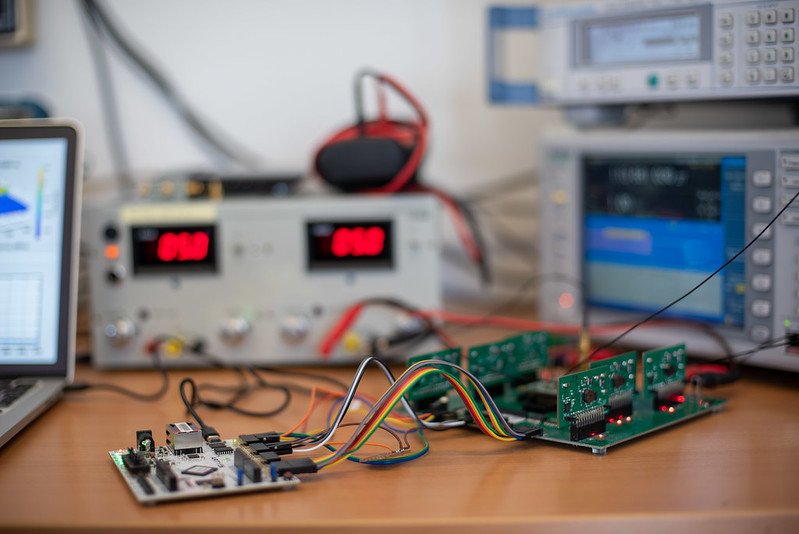
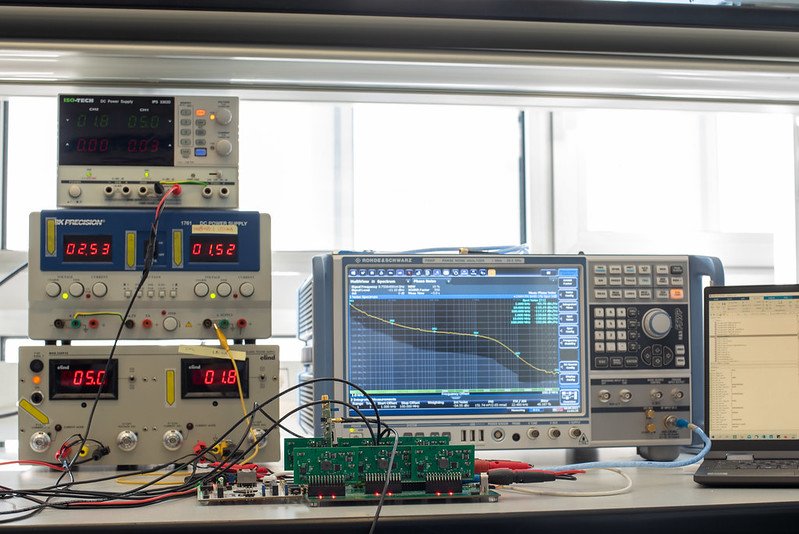
The lab makes use of last-generation servers and workstation, and professional CAD tools to design analog, mixed signal and digital circuit and systems (Cadence®, Mentor® and Synopsys® design flow) and millimeter-wave passives (Keysight®, Ansoft®, and Integrand® simulators), as well as equipment for measurements from DC to radio-frequency and millimeter-wave frequencies (Spectrum and Vector Signal Analyser up to 44GHz and 1GHz demodulation bandwidth, Signal Generators up to 6GHz with programmable modulations, Network Analyser fino a 40GHz, Oscilloscopes, Low-noise Power Supplies).
Service information
The lab is located in the building 22, floor 4th - Via Golgi 40 – Milano.